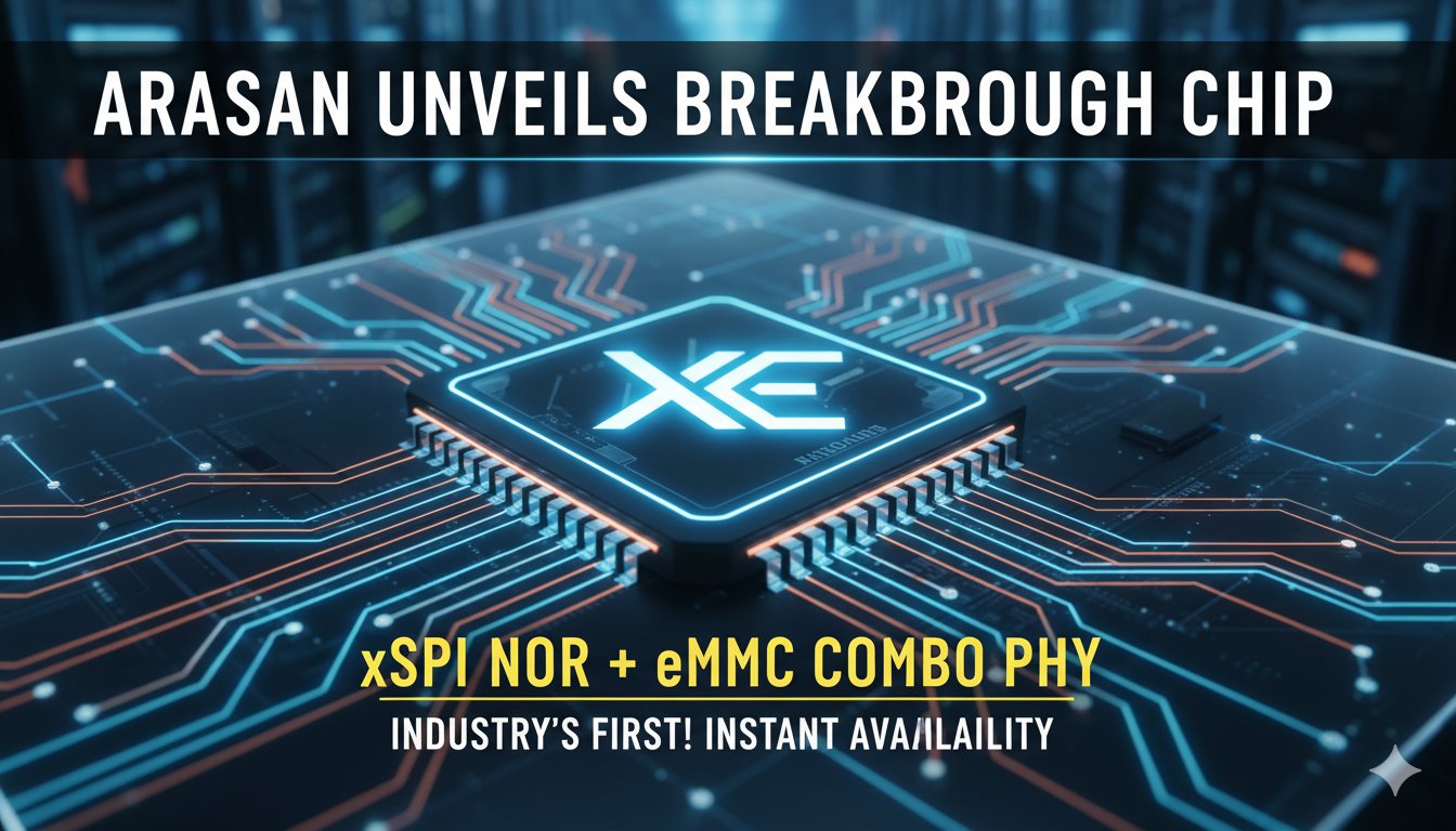
“Arasan’s latest innovation integrates xSPI for NOR Flash and eMMC for NAND Flash into a single PHY IP, targeting defense, aerospace, and medical sectors with reduced pin counts, lower costs, and seamless controller compatibility, now available across advanced foundry nodes from 28nm to 3nm.”
In the rapidly evolving semiconductor landscape, Arasan Chip Systems has positioned itself at the forefront by launching a pioneering intellectual property solution that addresses key challenges in system-on-chip designs. This new Combo PHY IP combines the capabilities of xSPI, which supports NOR Flash for reliable boot and code execution, with eMMC, enabling NAND Flash for high-density storage. The integration allows SoC manufacturers to handle both memory types through a unified physical layer, streamlining hardware requirements and optimizing performance in constrained environments.
The Combo PHY stands out for its shared I/O and analog front-end architecture, which significantly minimizes the number of pins needed—often a critical factor in compact, power-sensitive devices. By consolidating these interfaces, designers can achieve up to a 30% reduction in silicon area compared to deploying separate PHYs, directly translating to lower manufacturing costs and improved yield rates. This efficiency is particularly valuable in markets where every square millimeter of die space counts, such as in embedded systems for unmanned aerial vehicles or satellite communications.
From a technical standpoint, the IP adheres to stringent JEDEC standards: JESD251 for xSPI and the eMMC 5.1 specification. It supports high-speed operations, including HS400 mode in eMMC with a double data rate clock up to 200MHz, and xSPI-400 mode with similar clock speeds. This ensures data transfer rates that meet the demands of real-time processing in mission-critical applications, where latency can compromise system integrity.
| Feature | xSPI Mode (NOR Flash) | eMMC Mode (NAND Flash) |
|---|---|---|
| Protocol Compliance | JESD251 | eMMC 5.1 |
| Max Clock Speed | 200MHz DDR | 200MHz DDR (HS400) |
| Data Rate | Up to 400 MB/s | Up to 400 MB/s |
| Key Benefits | Fast boot, code execution reliability | High-density bulk storage, cost efficiency |
| Shared Components | I/O pads, analog DLL for PVT compensation | I/O pads, analog DLL for PVT compensation |
The table above highlights the dual-mode capabilities, underscoring how the Combo PHY provides flexibility without sacrificing speed or compatibility. Protocol switching can be managed via software or hardware controls, allowing dynamic adaptation based on application needs. Additional features include built-in multiplexers for interface selection, differential receivers for noise immunity, and configurable drive strengths (ranging from 33ohm to 100ohm) to match various board layouts.
Market Implications and Adoption Potential
This release comes at a time when the global semiconductor IP market is projected to exceed $10 billion by 2030, driven by demands from AI, edge computing, and autonomous systems. Arasan’s solution is poised to capture a share of this growth, particularly in the defense and aerospace segments, where U.S. Department of Defense spending on advanced electronics continues to escalate amid geopolitical tensions. Companies developing SoCs for radar systems, avionics, or secure communications can leverage this IP to reduce bill-of-materials costs by 15-20%, based on integrated design efficiencies.
In the broader electronics ecosystem, the Combo PHY aligns with trends toward heterogeneous integration, where mixing NOR and NAND memories in a single package enhances overall system resilience. For instance, NOR Flash’s instant-on capability complements NAND’s scalability, making the IP ideal for hybrid storage in medical imaging devices or industrial IoT controllers. Early adopters in these fields could see accelerated time-to-market, with Arasan claiming up to a 25% reduction in development cycles due to the pre-verified, silicon-proven nature of the IP.
Technical Deep Dive: Architecture and Implementation
Delving deeper, the PHY incorporates an analog delay-locked loop (DLL) that maintains precise clock delays across process, voltage, and temperature variations, ensuring stable operation in harsh environments like those encountered in aerospace applications. The I/O design supports both push-pull and open-drain transmitters, with the former offering multiple impedance options to optimize signal integrity and power consumption.
Testability is another strong suit, with built-in self-test (BIST) features and DC-testing modes for I/Os, facilitating easier validation during chip fabrication. Analog DLL phase measurements further aid in debugging, reducing the risk of field failures in high-stakes deployments.
For integration, Arasan provides a comprehensive deliverables package, including GDSII layouts, Verilog models, IBIS simulations, and gate-level netlists with scan insertion for design-for-test. This turnkey approach minimizes integration hurdles, allowing fabless semiconductor firms to focus on core innovations rather than peripheral interface challenges.
Strategic Positioning in the IP Landscape
Arasan’s track record bolsters the credibility of this release. With over a billion chips incorporating its IP in circulation, the company has established dominance in mobile storage solutions, including UFS and NAND controllers. This Combo PHY extends that expertise into emerging standards like xSPI, which is gaining traction as a successor to traditional SPI for faster, more efficient NOR interfaces.
In terms of competitive edge, the unified design differentiates it from fragmented offerings where separate PHYs inflate costs and complexity. This could pressure rivals to accelerate their own combo solutions, potentially sparking a wave of consolidation in the IP provider space. For U.S.-based manufacturers, relying on domestically developed IP like Arasan’s enhances supply chain security, aligning with national initiatives to bolster semiconductor self-sufficiency.
Applications Across Sectors
Beyond defense and aerospace, the IP finds relevance in automotive electronics, where reliable boot mechanisms are essential for advanced driver-assistance systems. In consumer devices, it could enable slimmer profiles for wearables or smart home hubs by optimizing storage interfaces. Medical applications, such as portable diagnostic tools, benefit from the combo’s ability to securely store patient data while ensuring quick access to firmware.
Overall, this IP represents a strategic pivot toward multifunctional designs that cater to the increasing complexity of modern SoCs, where balancing performance, power, and cost is paramount.
Disclaimer: This article is for informational purposes only and does not constitute financial advice, investment recommendations, or endorsements. All information is based on publicly available data and industry reports; readers should conduct their own research and consult professionals before making decisions.